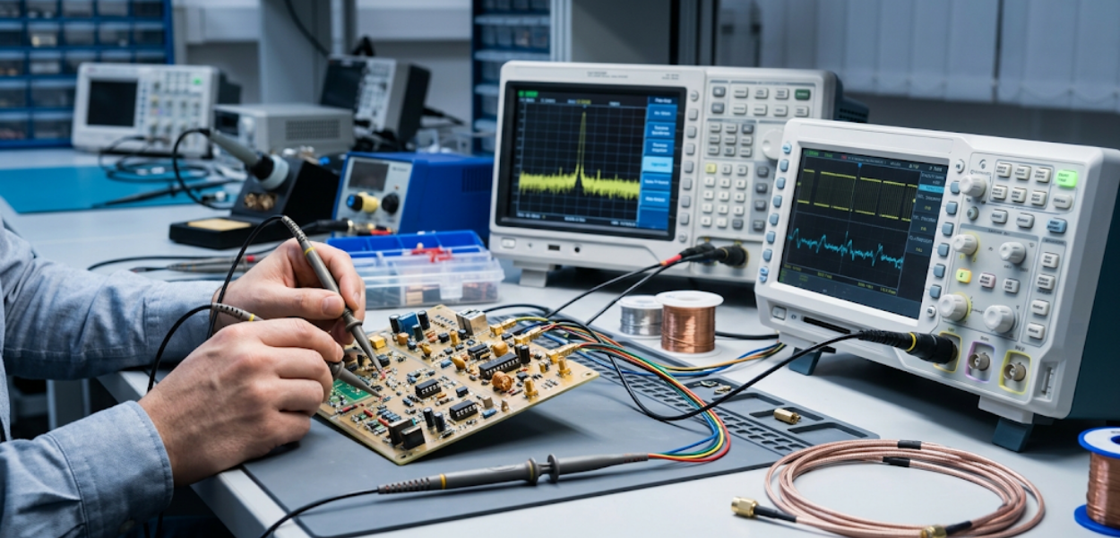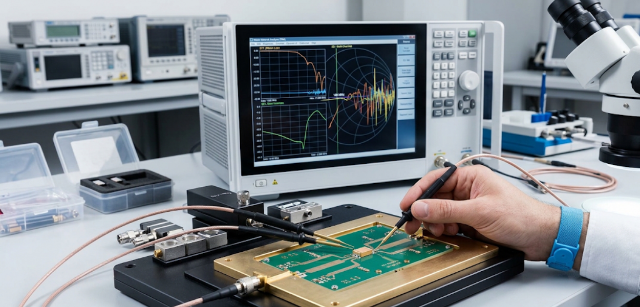

Digital design teams need more than just knowledge of HDL syntax. They need to understand how hardware specifications translate into register-transfer-level logic, how synthesis turns that logic into resources inside FPGA chips, and how verification confirms that the resulting design actually works as required.
What Problem Does an Integrated Training Path in This Field Solve?
Weak skills at any stage inevitably lead to downstream problems - poor register-transfer-level architectures produce inefficient hardware, weak testbench development lets functional bugs go undetected, incorrect timing constraints cause implementation failures, and limited knowledge of FPGA resources leads to inefficient use of lookup tables, registers, and memory.
An integrated training path connects digital design theory to practical engineering activities - HDL development, register-transfer-level modeling, simulation, synthesis, timing analysis, verification, and FPGA implementation - all in one connected sequence, instead of separate exercises disconnected from each other.
Why Should the Curriculum Follow a Sequence From Theory to Implementation?
The logical sequence reflects the interdependence between technical competencies - trainees first need to understand digital logic and FPGA architecture before they can make informed decisions in register-transfer-level design. They then need HDL skills before developing synthesizable designs. After a design is created, simulation and testbenches provide functional verification, synthesis shows how the description translates into hardware structures, and timing constraints determine whether the implementation meets performance requirements.
This approach lets trainees actually identify the source of a design problem - a simulation failure may point to an issue in the register-transfer-level design, a synthesis result may reveal inefficient coding, and a timing violation may require architectural adjustments. This diagnostic ability is critical in real professional engineering environments.
What Technical Skills Do Trainees Develop?
Digital design architecture is the first area - combinational and sequential logic, synchronous systems, registers, datapaths, and finite state machines. Next come VHDL and Verilog - entities, architectures, modules, ports, signals, operators, and procedural blocks.
After that comes register-transfer-level design - representing functional requirements using registers, data movement, and control structures. Then FPGA architecture and lookup tables - lookup tables, registers, memory resources, and computational resources, and connecting register-transfer-level structures to the hardware they actually map to.
Verification happens through developing testbenches and simulations - providing controlled inputs, defining expected behavior, and catching design errors before hardware deployment. Synthesis training shows how register-transfer-level descriptions translate into implementable hardware, and timing training covers clock definitions, input/output constraints, and setup and hold requirements.
How Is Trainees' Ability to Apply This in Practice Demonstrated?
Assessment starts with individual technical exercises - producing HDL structures, creating register-transfer-level modules, and demonstrating expected functional behavior through simulation. Testbench assignments provide evidence of verification ability - creating suitable stimuli, evaluating outputs, and identifying differences between expected and actual behavior.
Synthesis activities provide a second assessment point - reviewing the resulting hardware structures and resource reports, and identifying opportunities to improve resource utilization. Timing exercises measure the ability to identify and interpret timing constraints. The final practical project provides integrated assessment - the trainee must move through multiple stages of the entire design development cycle, not just complete separate exercises.
How Is This Training Practically Delivered to Corporate Teams?
Workshops are well suited to introducing complex concepts such as register-transfer-level architecture, synthesis, and timing analysis. Online training supports distributed teams, allowing participants to study language structures and digital design principles flexibly. Hands-on lab sessions are critical, because gaining the ability to work with FPGAs depends on actual practice - trainees need opportunities to write designs, run simulations, and examine synthesis results.
Hybrid training combines scheduled instructor sessions with independent exercises, which helps organizations whose employees are spread across multiple locations. On-site training can be organized around the organization's technical environment and its actual project requirements.
What Professional Outcomes Should Organizations Measure?
Managers should measure the quality of register-transfer-level development, simulation errors, debugging time, synthesis warnings, timing violations, FPGA resource utilization, and implementation success - course completion alone does not prove organizational impact, so baseline indicators must be defined before training begins.
For register-transfer-level teams, useful indicators include development time and code review results, and for verification teams, simulation errors and testbench effectiveness can be measured. Synthesis results provide technical evidence through resource utilization and warnings, and timing performance is evaluated through the number and severity of unresolved timing violations.
How Does This Path Apply to Different Organizational Roles?
Digital design engineers can develop their register-transfer-level and HDL capabilities, and FPGA engineers can focus on synthesis, timing, implementation, and resource management. Embedded systems specialists can understand how programmable hardware integrates with overall system architectures. Communications teams can use these skills in systems involving specialized digital signal processing, and industrial automation teams can apply the concepts to real-time control and processing environments.
Conclusion
Completing an integrated path like this demonstrates that the trainee has developed a structured understanding of digital hardware description, and can apply HDL, register-transfer-level, verification, synthesis, timing analysis, and FPGA implementation concepts together - not just disconnected theoretical knowledge. The final practical project provides a real opportunity to demonstrate the full sequence from specification to implementation and verification.