Analog electronics and RF circuits don't behave the way digital systems do. Below 100 MHz, a resistor behaves like a resistor and a wire behaves like a wire. Above that threshold, parasitic inductance, parasitic capacitance, and transmission-line effects take over. Engineers who design without accounting for this shift produce circuits that fail in the lab, even when every component meets its datasheet specification.
Why Do Components Stop Behaving According to Their Datasheet Values Above 100 MHz?
Above 100 MHz, the parasitic inductance and capacitance in real components become comparable in magnitude to their intended values, so a resistor, capacitor, or inductor no longer behaves as a single ideal element, but as a network of parasitic reactive elements. A 100-ohm resistor can show impedance 30% higher or lower than its nominal value at 500 MHz, depending on the package geometry. Surface-mount packages reduce this effect compared to through-hole components, because shorter leads mean less parasitic inductance.
Capacitors show a related but inverse pattern - every real capacitor has an equivalent series inductance caused by its leads, which combines with the intended capacitance to create a self-resonant frequency. Below that frequency, the component behaves as a capacitor, and above it, it behaves as an inductor. Circuit designers choosing a bypass capacitor for an RF stage operating at 900 MHz need to select a package and value whose self-resonant frequency is close to the operating frequency, not just the value that satisfies the calculation at low frequency.
How Does Transistor Behavior Change at RF Frequencies?
Transistor gain decreases with frequency because internal junction capacitances create feedback paths that had negligible effect at lower frequencies, which reduces usable gain and shifts the optimal bias point for stable operation. Every transistor has a frequency at which current gain drops to unity, called the transition frequency. Below one-tenth of that frequency, a transistor stage behaves close to its low-frequency model, but near the transition frequency, base-to-collector capacitance feeds the signal back from output to input, reducing gain and introducing phase shift that can cause instability.
Biasing networks need different handling at RF frequencies - RF transistor stages typically separate the DC bias path from the signal path using RF chokes and bypass capacitors. Errors in this separation are one of the most common causes of oscillation in amplifier stages that otherwise meet every DC specification. Operational amplifiers face a similar constraint - the gain-bandwidth product determines the trade-off between closed-loop gain and usable bandwidth.
Why Does Impedance Matching Become Critically Important Above 100 MHz?
Signal wavelengths shrink to dimensions comparable to circuit trace lengths, which turns ordinary board traces into transmission lines, where impedance mismatch causes signal reflections and power loss. At 1 MHz, the signal wavelength is 300 meters, and at 1 GHz it's only 30 centimeters. When board trace lengths approach one-tenth of the wavelength, the trace stops behaving as a simple conductor and starts behaving as a transmission line with its own characteristic impedance.
Reflected power reduces the signal reaching its intended destination, and can create standing waves that distort amplitude across the circuit. Engineers measure this using voltage standing wave ratio - a 2-to-1 ratio corresponds to roughly 11% of incoming power reflecting back instead of reaching the load. Correcting this requires impedance-matching networks built from combinations of inductors and capacitors, and at higher frequencies, sections of transmission line with specific electrical lengths.
How Does Noise Behave Differently in RF Circuit Stages?
Noise figure becomes the dominant design constraint at RF frequencies, because every amplifier stage adds noise that accumulates according to the Friis equation - meaning the first stage in a receiver chain determines the noise floor for the entire system. Noise figure expresses how much a component or stage degrades the signal-to-noise ratio as a signal passes through it, and it's measured in decibels.
This is why front-end RF design prioritizes a low-noise amplifier as the first active component after the antenna, even if later stages use lower-cost, higher-noise components. Improving the front-end noise figure by just one decibel can improve receiver sensitivity by a proportional amount, which directly affects range and reliability in wireless systems.
What Role Does Filter Design Play in High-Frequency Circuit Performance?
Filter design at RF frequencies separates desired signals from noise, harmonics, and interference from adjacent channels, using passive networks whose component values and structure are chosen specifically for the frequency range and the required attenuation. RF filters typically use multi-stage networks of inductors and capacitors, or at microwave frequencies, distributed elements such as stripline resonators.
A component's quality factor (Q) determines how closely a real filter approaches its theoretical response - inductors with low quality factor introduce passband loss and blur the sharpness of the filter's cutoff. This is why RF filter design often favors capacitor-based structures wherever possible, because they are easier and less costly at RF frequencies.
How Do Organizations Build High-Frequency Design Capability Within Their Teams?
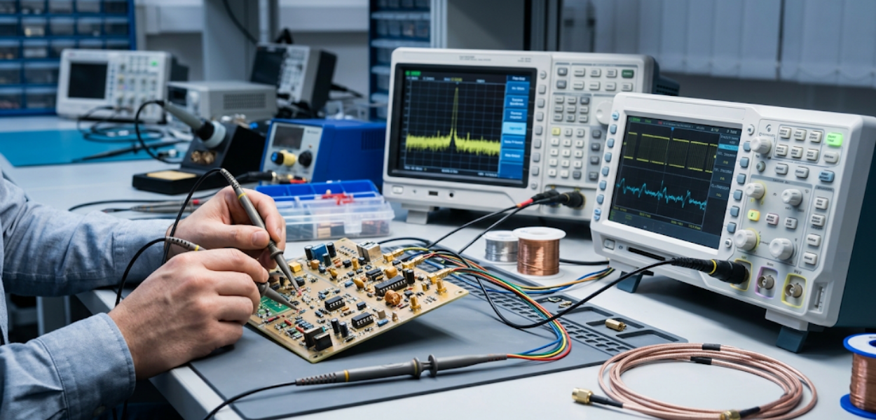
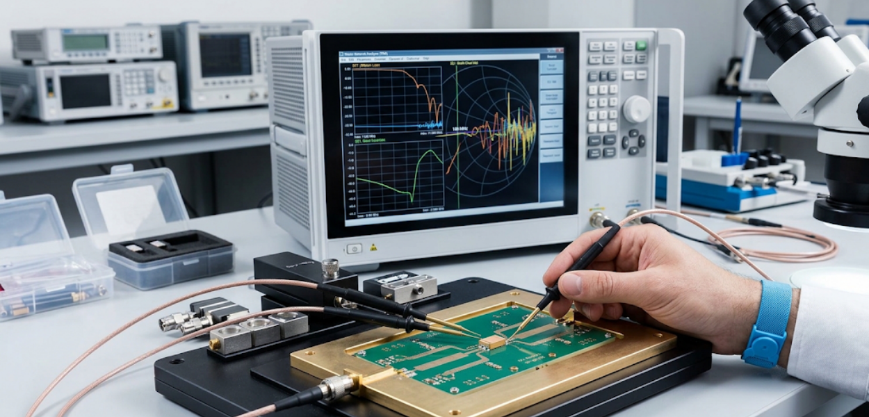
Building this capability requires structured, hands-on training that combines circuit theory with measurement practice, because RF design errors are hard to diagnose from simulation alone, and require engineers capable of directly interpreting network analyzer and spectrum analyzer data. Parasitic values vary by manufacturer, batch, and even component placement on the board, and engineers who rely entirely on simulation without measurement experience often produce designs that succeed in simulation but fail on the test bench.
Teams that lack dedicated RF training often route high-frequency problems to a small number of experienced engineers, which creates a bottleneck that slows product development and increases dependency risk when those engineers leave. Structured training distributes this capability across the whole team, which reduces reliance on a single point of failure and shortens the diagnostic cycle when a board fails to meet specification.
Conclusion
The delivery model matters as much as the content itself - cohort-based training with hands-on lab sessions produces stronger knowledge retention compared to self-paced video content alone, especially for skills that depend on interpreting actual measurement equipment. The gap between calculated behavior and measured behavior is exactly where most high-frequency design failures originate, which is what makes direct, hands-on experience at the test bench essential, not just theoretical instruction.